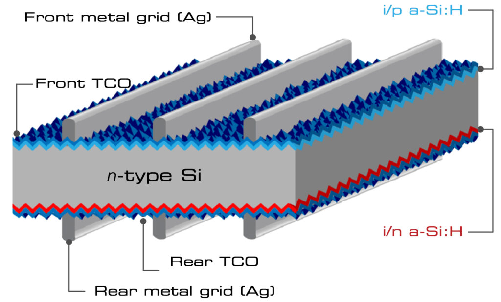
What is HJT Technology?
- HJT solar cells have double-sided structure design which can absorb incident light and scattered light from both sides, using a PECVD, very thin silicon intrinsic passivation layer and P-type silicon doped layer are formed on the top side of wafer-type monocrystalline silicon N after texturing and surface cleaning, then on the other side a very thin intrinsic silicon passive layer and N-type silicon doped layer is deposited.
- After deposition of amorphous silicon layer stacks, PVD magnetron sputtering coating technology is applied to deposit transparent oxide conductive film (TCo) and metal stack on both sides of the cells.
- Finally, the metal grids on both sides are formed by our innovative metallization technology.
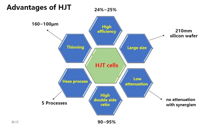
Advantages of HJT Technology
- High efficiency
- Large size
- Low attenuation
- High double-sided ratio
- Less process
- Hinning
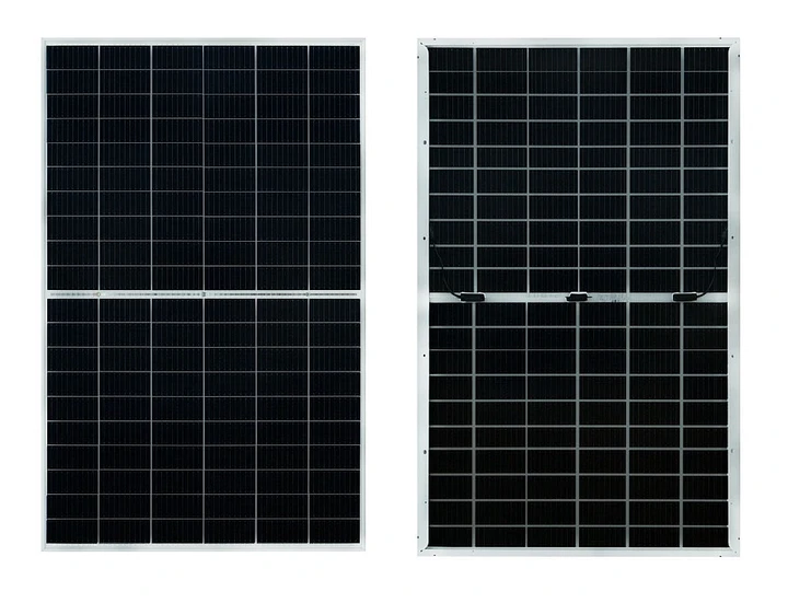
HJT Photovoltaic Modules
- Using a high efficiency heterojunction solar cell, up to more than 21.5% module efficiency.
- Leading Half-cut HJT cell technology.
- The more stable feed temperature coefficient of -0.24% results in a stable yield gain.
- Using N-type wafer, no LID caused by B-O pair
- Excellent PID resistance.
- The 85% double-sided factor brings greater yield gain from back to back.
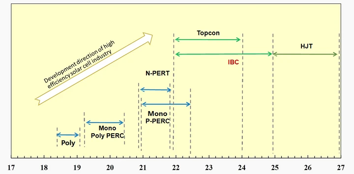
Development Direction Of High Efficiency Solar Cell Industry
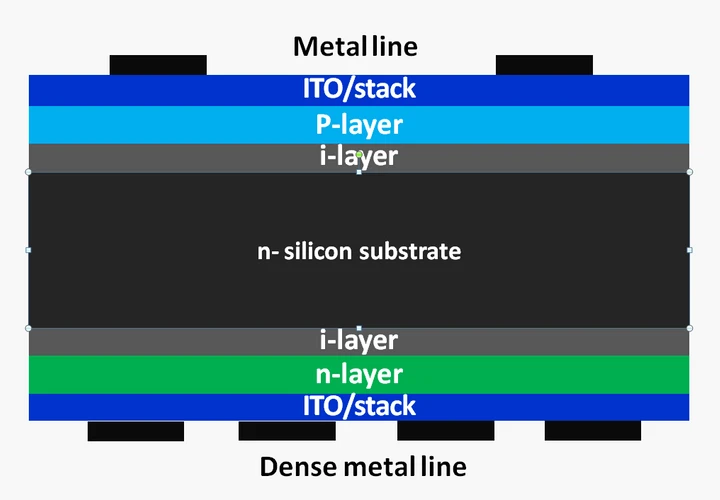
The HJT Technology Structure Diagram
Following such confusing times, people often find themselves locked up in a dilemma on the decision of installing the appropriate PV module for their homes, offices, etc. And for that very reason, we are here ready to assist you in whatever you need. Contact us now at Whatsapp: +86 159 2091 1832 and get a quote.
Post Views: 4,703
